The journey from a single, hand-assembled component to a modern System-on-Chip (SoC) with over 100 billion transistors is perhaps the greatest engineering feat in human history. To understand where we are going with AI-driven design, we have to look back at how we moved from physical geometry to abstract logic.
1. The “Paper and Foil” Era: Where it All Began
The journey of modern chip design started not in a sterile cleanroom, but on a laboratory bench at Bell Labs in December 1947. The world’s first transistor was a remarkably “manual” invention—a crude assembly of plastic, gold foil, and a sliver of germanium, all held together by a simple paperclip-like wedge. In those early days, there were no simulation tools or automated layouts; circuits were conceived as hand-drawn schematics on paper, where every connection was a physical wire and every “logic gate” was a visible, discrete component. This era of “paper drawings” required engineers to hold the entire complexity of a system in their heads, long before the first line of code or a single pixel of CAD software ever existed.
2. The Drafting Table and the X-Acto Knife
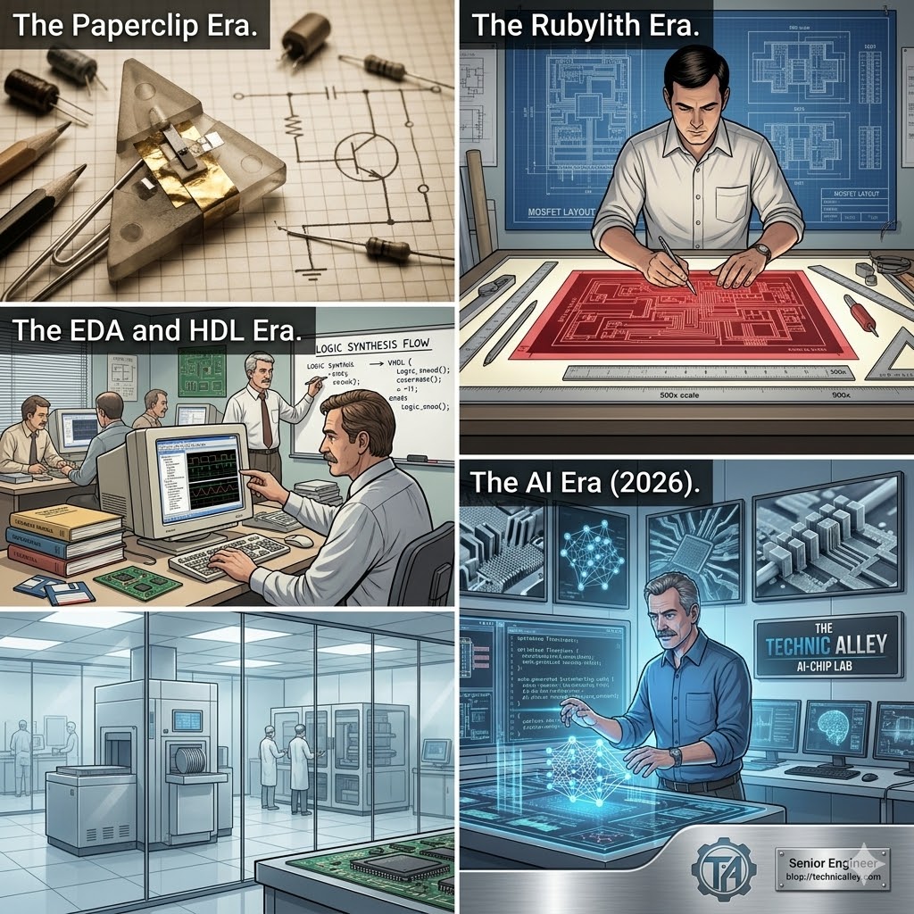
As transistors shrunk and integrated circuits (ICs) began to hold dozens, then hundreds of components, chip design moved to giant drafting tables. This was the era of Rubylith—a specialized two-layer plastic film (one clear, one red) that served as the master template for the chip’s layers. Engineers would painstakingly draw the circuit at 500x its actual size, and technicians would use X-Acto knives to cut away the red film to create the “masks” for the silicon.
It was a purely geometric process; a mistake of a fraction of a millimeter on a giant light table could mean a dead chip in the cleanroom. By the late 1970s, as designs approached 10,000 transistors, this manual drafting reached a “Complexity Wall.” It was no longer humanly possible to cut, check, and verify these patterns without a high probability of catastrophic error.
3. The Mead-Conway Revolution: Decoupling Physics from Logic
By 1980, the breakthrough came with the work of Lynn Conway and Carver Mead. Their seminal textbook, Introduction to VLSI Systems, proposed a radical shift: decoupling the design from the fabrication. They introduced three concepts that underpin the industry today:
- Lambda-Based Design Rules ($\lambda$): Instead of absolute measurements in microns, they defined rules based on a scaling factor, $\lambda$. This allowed a design to be “shrunk” to a newer process without being entirely redrawn.
- The Foundry Model: By creating a clean “interface” between the designer and the manufacturer, they birthed the fabless semiconductor industry.
- Structured, Hierarchical Design: They moved toward modularity, creating “Leaf Cells” (like an inverter or flip-flop) that could be snapped together like LEGO bricks.
4. Design Entry and the Schematic Era
As more complex chips became possible, companies began developing Application-Specific Integrated Circuits (ASICs). This created a need for efficient design entry. Schematic Entry tools soon became popular. At the time, the divide was clear: if you designed with languages like C, you were a software engineer; if you used a schematic editor, you were a hardware engineer.
The schematics were so intuitive that there was soon a demand for hierarchical designs and block generators. I once spoke with a senior hardware manager who insisted, “No hardware engineer will do any design using a language,” as his team struggled with the early days of VHDL. He couldn’t imagine a world where “writing” replaced “drawing.”
5. The Language Leap: VHDL and Verilog
Complexity eventually made schematics impossible to manage. Hardware Description Languages (HDL) like VHDL and Verilog gained dominance because they allowed for Logic Synthesis—automatically turning code into gates.
This pushed the industry toward powerful simulation and validation tools. We moved from simple testbenches to object-oriented platforms that generated constrained-random stimulus. Physical design tools also evolved to handle Design for Testing (DFT) and manufacturability, ensuring these billion-transistor webs could actually be mass-produced and tested.
6. The Era of Code Generation
While SystemVerilog is the workhorse of the industry, it often lacks the high-level abstraction of languages like C++ or Java. Designers got creative, using Perl and Python to create “HDL Generators.” Instead of coding every signal, we began writing scripts that built the hardware description for us, allowing us to manage even greater levels of abstraction.
7. AI: The New Frontier
As with everything in 2026, AI offers uniquely new ways to design hardware. We are moving beyond simple code generation into a frontier where AI can:
- Generate RTL and documentation from high-level “specs.”
- Automate fault detection and build autonomous test environments.
- Optimize physical layouts in hours that used to take weeks of human effort.
Conclusion
From a paperclip and gold foil to AI-generated silicon, the evolution of chip design is a story of humans building better tools to manage the chaos of our own progress. We are no longer just “drawing” chips; we are “teaching” machines how to build themselves.
