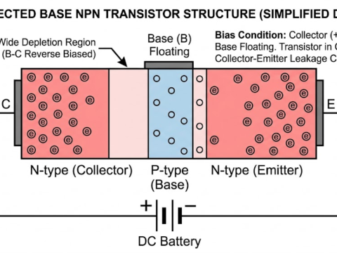
If you’re delving into electronics, one of the most fundamental semiconductor components you’ll encounter is the diode. Think of a diode as a one-way street for electricity—it allows current to flow easily in one direction but severely restricts it in the opposite direction.
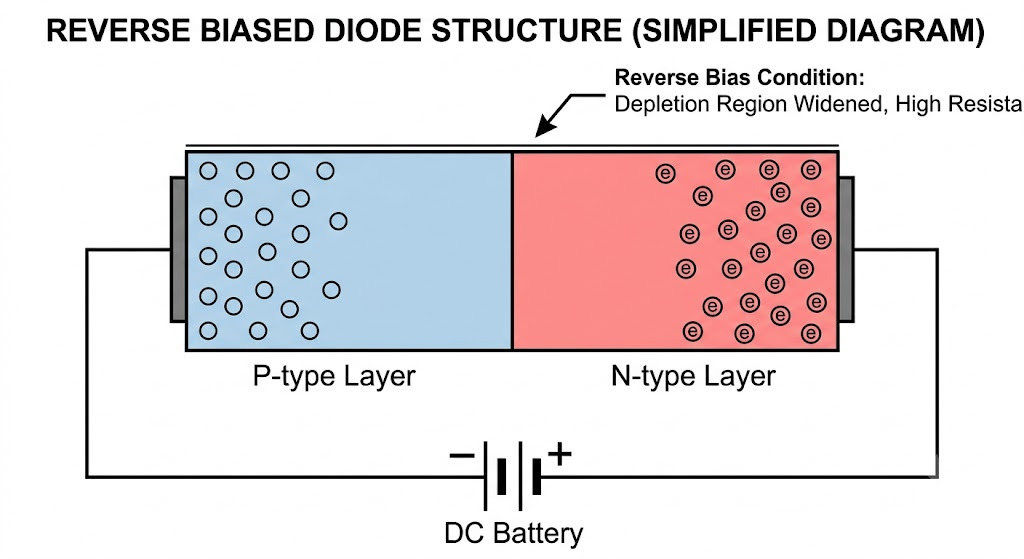
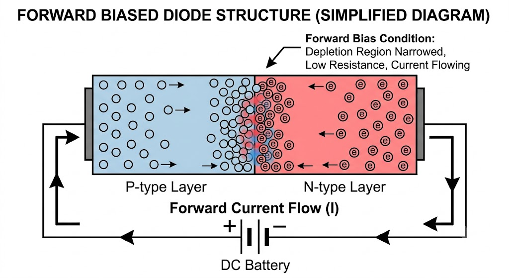
Let’s look at what is actually happening inside the P-N junction using a simplified structural diagram. In these diagrams, the P-type layer is represented in blue (containing positively charged “holes” shown as empty circles), and the N-type layer is in red (containing negatively charged electrons shown as circles with an ‘e’).
1. The Blocking State: Reverse Bias
First, let’s look at what happens when a diode prevents current from flowing. This is known as a Reverse Bias condition.
How it works:
- The Setup: The positive terminal of the DC battery is connected to the N-type layer, and the negative terminal is connected to the P-type layer.
- The Physics: Because opposites attract, the negatively charged electrons (‘e’) in the N-type layer are pulled away from the center junction toward the positive battery terminal. Simultaneously, the positively charged holes (empty circles) in the P-type layer are pulled toward the negative terminal.
- The Result: The charge carriers are pulled to the outer edges. This creates a wide “depletion region” in the middle—an area stripped of free charge carriers. This wide gap acts as a high-resistance barrier, effectively blocking any forward current from flowing.
2. The Conducting State: Forward Bias
Now, let’s flip the battery around and see how a diode conducts current. This is known as a Forward Bias condition.
How it works:
- The Setup: The battery is reversed. The positive terminal is now connected to the P-type layer, and the negative terminal is connected to the N-type layer.
- The Physics: Like charges repel. The positive terminal repels the holes in the P-type layer, pushing them toward the center junction. The negative terminal pushes the electrons in the N-type layer toward the center as well.
- The Result: The holes and electrons are forced together and mix right at the junction. The depletion region is squeezed down to almost nothing. With the barrier gone, the diode acts as a low-resistance path, allowing a continuous forward current (I) to flow freely through the circuit.
Summary: Whether you are building a simple logic gate or working with high-voltage rectification, it all boils down to how these charge carriers interact at the P-N junction. By simply changing the polarity of the applied voltage, you dictate whether the diode acts as an open switch or a closed path!