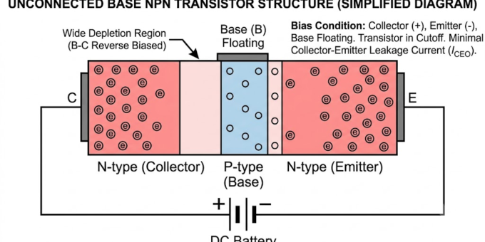
The humble NPN bipolar junction transistor is a semiconductor giant, the heart of modern electronics. Often simplified as a voltage-controlled switch, its power truly lies in its ability to operate in three distinct modes, transforming from a precise control valve to a saturated switch and even a complete open circuit. To truly master electronics, you must master the NPN’s operating states.
We’ll break down the physics and visuals of these three states—Active Mode (Control), Saturation (fully ON), and Cutoff (fully OFF)—using detailed, simplified diagrams.
Mode 1: The Control Valve – Active Mode (Diagram 1)
In its most linear form, the NPN transistor is an amplification device. We call this Active Mode. Think of it as a precisely controlled valve on a water pipe.
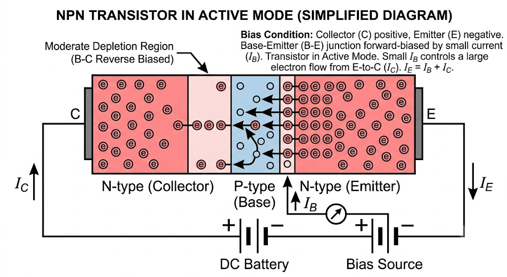
How it works (Visualizing Diagram 1):
- The Setup: The Base-Emitter (B-E) junction is forward-biased (like a diode turned on) by the smaller ‘Bias Source’, and the Base-Collector (B-C) junction is reverse-biased (like a diode turned off) by the main ‘DC Battery’.
- The Physics:
- A small Base current ($I_B$) is carefully injected into the base, pushing a manageable number of electrons across the narrow P-type Base layer.
- Most of these electrons, instead of recombining with holes in the base (the few open circles), are swept right across the moderate depletion region at the reverse-biased B-C junction and collected by the large, high-energy Collector.
- The Result: A small control current ($I_B$) modulates a far larger current ($I_C$) flowing through the main Collector-Emitter path. The output current $I_C$ is directly proportional to the input current $I_B$ (controlled by $\beta$ or $H_{FE}$). This is how analog signals are amplified. Look closely at the diagram: a small trickle in, and a massive flow out.
Mode 2: The Saturated Switch – Saturation (Diagram 2)
Flipping our conceptual valve completely open transforms the transistor into its fully ON state: Saturation. In this mode, the transistor acts as a closed switch, limited only by the external circuit itself.
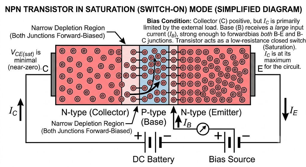
How it works (Visualizing Diagram 2):
- The Setup: We dramatically increase the output of the ‘Bias Source’. The B-E junction remains forward-biased, but the main ‘DC Battery’ also pulls hard enough to overcome the barrier, making the B-C junction also forward-biased.
- The Physics (A Packed Scene):
- A massive, heavy current of electrons ($I_B$) is driven into the base, swamping all available holes.
- The N-type Collector and Emitter layers are packed densely with charge carriers (the ‘e’ count is vastly increased).
- The central junction barriers are squeezed to a minimum, creating a very narrow, high-conductivity path. It looks like a crowded, almost solid wall of moving charges.
- The Result: The transistor is fully ON, conducting maximum current ($I_C$ and $I_E$) for the given load. $I_C$ is no longer controlled by $I_B$; the output current is at its maximum and is primarily limited by the external load and the main ‘DC Battery’ voltage. The Collector-to-Emitter voltage drop ($V_{CE(sat)}$) is minimal.
Mode 3: The Broken Pipe – Cutoff (Diagram 3)
The true OFF state is Cutoff. No control current, no power flow. It is the ultimate electronics non-conducting state, like a physical disconnect.
How it works (Visualizing Diagram 3):
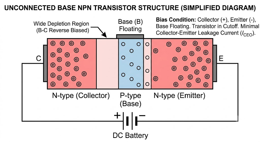
- The Setup: The connection to the ‘Bias Source’ is completely broken or turned off (the meter reads zero). The circuit has $I_B = 0$.
- The Physics (A Barren Landscape):
- With no base current to push electrons, both the B-E and the B-C junctions are now reverse-biased.
- The charge carriers in all layers are recessed and sparse (minimal ‘e’ count), showing a barren, inactive state.
- The depletion regions at both junctions are now very wide (see the labels pointing to the massive central barriers). These wide empty gaps form impenetrable high-resistance barriers.
- The Result: Zero significant current flows from Collector to Emitter. The transistor acts as a fully open switch, blocking all current path. The entire voltage of the main DC Battery appears across the Collector-Emitter junction ($V_{CE}$ is high).
Summary and Application
These distinct modes enable transistors to be versatile.
- Active Mode: Amplifying weak signals (radio, microphones) and analog control.
- Saturation Mode: Fully switching a circuit element ON (motors, relays, LEDs).
- Cutoff Mode: Fully turning a circuit element OFF (preventing power flow).
By understanding the physics and the visual state of the junctions—from narrow and dense barriers (ON) to wide and lifeless ones (OFF)—you can diagnose any NPN circuit application and harness the true power of this incredible semiconductor device.